Popular Headlines
 IT job growth in 2025: 5 ways to advance your tech career
Explore the tech certifications, emerging technologies, and leadership paths that can drive your IT career forward in 2025 and specific actions you can take now.
IT job growth in 2025: 5 ways to advance your tech career
Explore the tech certifications, emerging technologies, and leadership paths that can drive your IT career forward in 2025 and specific actions you can take now.
- What is the C# programming language? Originally called Cool, C# was invented by Microsoft’s Anders Hejlsberg and launched in July of 2000. C# was designed from the ground up to suit both hosted and embedded systems. For example, C# can run both on your desktop computer and on an IoT dev
- How to use AWS Glue crawlers with Amazon Athena As a data professional, you deal with immense amounts of data from a variety of sources. This can make data management and analysis a challenge. Luckily, two AWS services can help: AWS Glue and Amazon Athena. When you integrate these services, yo
- How to install Python: The complete Python programmer's guide An easy guide on how set up your operating system so you can program in Python, and how to update or uninstall it. For Linux, Windows, and macOS.
- IT skills you (and your tech teams) need to develop at work When tech changes, the skills an organization needs also change. As a technologist, what skills should you prioritize learning to build or boost your tech career? As a leader, how can you help your teams develop these skills through effective upskill
- A Full Guide to Using PHP Configuration Files for Best Practice In this article, we will cover how to set up a secure PHP configuration file. This article will be more helpful for custom coders.
Popular Topics
- Douyin level price list 1-75 Douyin level price comparison table: 1, level 1 = 0.5 yuan; level 2, 2 = 1 yuan; level 3, 3 = 2 yuan; level 4, 4 = 3 yuan; level 5, 5 = 5 yuan; 6, 6 Level = 7 yuan; Level 7 and 7 = 9 yuan; Level 8 and 8 = 13 yuan; Level 9 and 9 = 18 yuan; Level 10 and 10 = 24 yuan and so on. This topic provides you with relevant articles, downloads, and course content for you to download and experience for free.
- wifi shows no ip assigned Solution to wifi showing no IP allocation: 1. Restart the device and router, turn off the Wi-Fi connection on the device, turn off the device, turn off the router, wait a few minutes, then reopen the router to connect to wifi; 2. Check the router settings and restart DHCP, make sure the DHCP function is enabled; 3. Reset network settings, which will delete all saved WiFi networks and passwords. Please make sure they are backed up before performing this operation; 4. Update the router firmware, log in to the router management interface, and find the firmware Update options and follow the prompts. This topic provides you with various wifi-related articles, downloads and courses. I hope
- Virtual mobile phone number to receive verification code To receive the verification code with a virtual mobile phone number: first enter the Yima verification code receiving platform; then register as a website member; then open the SMS verification code service and select an operator; finally obtain the virtual mobile phone number, go to the platform where the verification code is to be sent, and put the phone Fill in the number and select [Send Verification Code].
- How to turn off windows security center Windows Security Center is a comprehensive security control panel for Windows systems, including firewall status prompts, anti-virus software status prompts, automatic update prompts and other basic system security information. So how to turn off Windows Security Center? I believe many friends are still not clear about it. PHP Chinese website has brought you relevant tutorials and tutorials. You are welcome to come and learn and read.
- myfreemp3 Myfreemp3 is a free online music search engine that allows users to search and play music directly on the web. Myfreemp3 has the advantages of fast search engine and rich resources. PHP Chinese website has compiled related articles and APP downloads about myfreemp3 for everyone. etc.
IntelligentAIQ&A
Ask

【Learning PHP】
PHP is a widely used open source multi-purpose scripting language. Compared with other technologies, PHP itself is open source and free; the program can be embedded in HTML for execution, and the execution efficiency is much higher than CGI that completely generates HTML tags. It runs on the server side, consumes very few system resources, has strong cross-platform and high efficiency features, and PHP supports almost all popular databases and operating systems. The most important thing is that PHP can also use C and C for program expansion. , PHP language has a very wide range of applications in WEB development. In addition, object-oriented has been greatly improved in PHP4 and PHP5, and can also be used to develop large-scale commercial programs.


- php array_diff_assoc() function
- php array_merge_recursive() function
- TCP/IP mail
- TCP/IP protocol
- TCP/IP addressing
- Web Forms - Database Connection
- Web Forms - ArrayList object
- Web Forms - Button control
- Web Forms - TextBox control
- Web Forms - HTML forms
- Web Forms - Events
- ionic Toggle
- ionic forms and input boxes
- ionic list
- ionic button
- ionic bottom
- ionic head
- MVC - Model
- MVC-SQL Database
- MVC - View
-

- IntermediateThe latest ThinkPHP 5.1 world premiere video tutorial (60 days to become a PHP expert online training course)
-
1415428 times of learning
- Free
-

- ElementaryPHP introductory tutorial one: Learn PHP in one week
-
4253729 times of learning
- Free
-

- ElementaryPHP complete self-study manual
-
2292065 times of learning
- Free
-

- ElementaryphpStudy quick entry video tutorial
-
515528 times of learning
- Free
- Hot
- New
- Follow
- web3.0
- Backend Development
- Web Front-end
- Database
- Operation and Maintenance
- Development Tools
- PHP Framework
- Daily Programming
- WeChat Applet
- Common Problem
- Other
- Tech
- CMS Tutorial
- Java
- System Tutorial
- Computer Tutorials
- Hardware Tutorial
- Mobile Tutorial
- Software Tutorial
- Mobile Game Tutorial


Here are a few question-based titles based on your article, keeping the focus on overriding `!important` styles:
* Can You Really Outsmart `!important` Styles? JavaScript Techniques to Override the U
Overriding the Unstoppable !important StyleWhile CSS's !important flag may seem all-powerful, it is not immune to the manipulation of JavaScript....
2024-10-27 23:17:29


Here are a few title options, depending on the emphasis you want to place:
Focus on the specific error:
* Why Am I Getting a \'PHP Fatal Error: Call to Undefined Function json_decode\' Des
PHP Fatal Error: Call to Undefined Function json_decodeThis error typically occurs when the JSON extension is not installed or enabled for PHP....
2024-10-27 22:36:30


The Top easons You Should NOT Use Ember.js on Your Next Project
If you're starting a new project and trying to decide on which frontend framework to use, then this article is for you. Here are my top 7 reasons not to use Ember.js on your next project.
1. You Aren't an Ambitious Web Developer
Ember mar
2024-10-27 21:30:02
More


Here are a few question-based titles based on your article, keeping the focus on overriding `!important` styles:
* Can You Really Outsmart `!important` Styles? JavaScript Techniques to Override the U
Overriding the Unstoppable !important StyleWhile CSS's !important flag may seem all-powerful, it is not immune to the manipulation of JavaScript....
2024-10-27 23:17:29


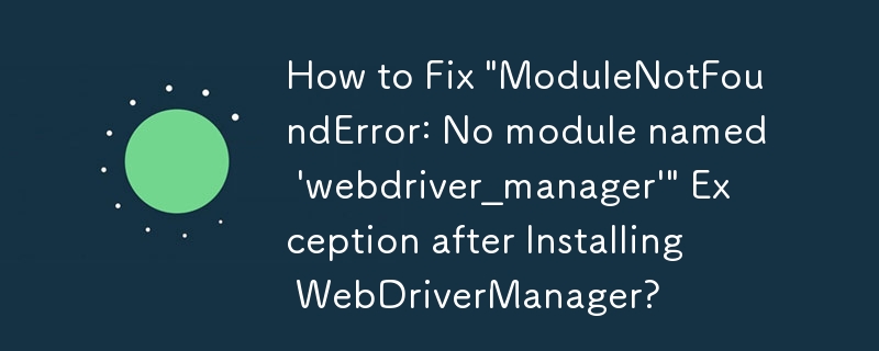
ModuleNotFoundError: No module named 'webdriver_manager' Even After Installing WebDriverManagerAfter installing WebDriverManager on Windows-10, errors still occur when trying to use it. For instance, the code below throws an "ModuleNotFoundError
2024-10-21 13:15:03