(Nweon September 26, 2023) Microsoft believes that Micro LED has the characteristics of small size, light weight, high brightness, and high packaging density, and may be particularly suitable for applications that require high resolution, small size, and light weight. weight of the head-mounted display.
In the patent application titled "Microlenses providing wide range chief ray angle manipulation for a panel display", Microsoft introduced a microlens that provides wide range chief ray angle manipulation for a panel display, and the configuration of the microlens Array display system.
Wherein, each microlens in the array corresponds to a respective pixel of the panel display. The configuration of the microlenses varies according to their distance from the central projection axis in the display plane of the panel. Microlenses can be configured as surfaces to increase optical efficiency.
To improve the uniformity of display illumination, microlenses can be used to adjust the emission angle of a specific pixel to match its chief ray angle CRA. In this way, the main ray of the pixel will pass through the pupil center of the projection optical system in the display system, thereby achieving a more uniform lighting effect
Microlenses with two different configurations can be used to shape light for on-axis pixels that are closer to the central axis relative to farther off-axis pixels. For off-axis pixels, the microlens configuration includes an asymmetric freeform lens surface to collimate light and match the CRA.
The original sentence can be rewritten as: The shapes of circular symmetric and asymmetric free microlenses can be combined with the spatial offset between the microlenses and corresponding pixels to achieve more accurate CRA matching
Microsoft pointed out that panel displays composed of respective Micro LED arrays and corresponding microlenses provide improvements in optical efficiency and illumination uniformity for projection display systems. Increased optical efficiency saves power, while improved lighting uniformity provides a more satisfying user experience
In addition, the wide range of CRA operation enabled by current microlens configurations can provide more design freedom for downstream components in the display system, such as making optical projection systems more compact, thereby reducing the size of the system using current microlens arrays. The size and weight of the headset.
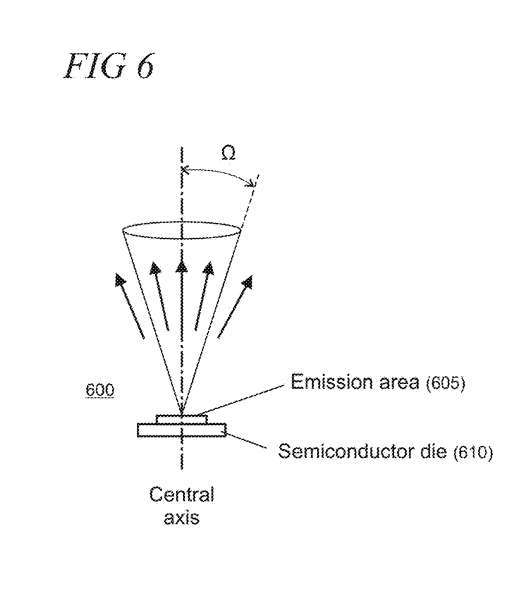
Figure 6 shows the cone angle Q for emitting light from an illustrative Micro LED 600 configured to emit monochromatic light, for example, for pixels or sub-pixels in panel display 320. The emitting area 605 of the semiconductor chip 610 in the Micro LED can take various shapes, including rectangular, circular, hexagonal, etc., to meet the requirements of a given application.
Not all light emitted from the emission area can effectively illuminate the panel display. For example, for projection-based display devices, only light emitted within the cone angle Ω=±10-15 degrees can successfully propagate to the downstream projection system
Therefore, light is lost after being emitted from the wide-angle emitter, resulting in a decrease in the optical efficiency of the display system. According to the method proposed by Microsoft, optical efficiency can be maximized by arranging microlens arrays on each pixel source of the panel display to collimate light to the central cone angle. This optimization can save energy
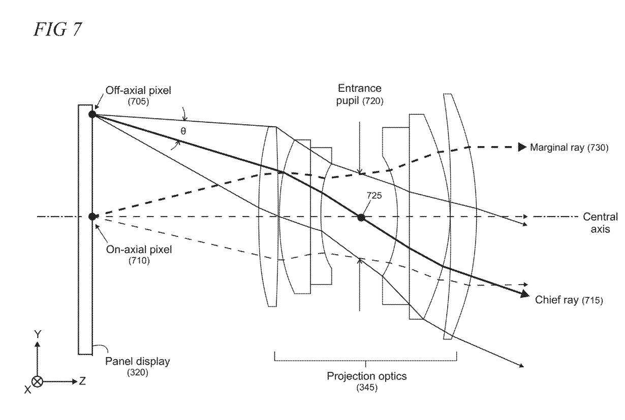
Figure 7 shows the chief ray angle θ. In this embodiment, the panel display and projection optics have a coaxial or telecentric configuration. However, a non-telecentric configuration may be used in alternative embodiments utilizing the present principles.
What needs to be rewritten is: The principal ray angle CRA describes the angle of the principal ray 715 traced between the point on the panel display 320 for the off-axis pixel 705 and the center of the pupil of the projection optic 345. In the figure, the pupil is denoted by reference number 720 and the center point is denoted by reference number 725. As shown, edge rays 730 pass from an axial pixel 710 in the center of the panel display to the maximum aperture of the pupil. Rewritten content: The chief ray angle CRA refers to the angle between the point of the traced chief ray 715 at the off-axis pixel 705 on the panel display 320 and the pupil center of the projection optical element 345 . The pupil in the figure is numbered 720, and the center point is numbered 725. As shown, edge ray 730 passes from an axial pixel 710 in the center of the panel display to the maximum aperture of the pupil
In a projection system, only the light closest to the principal ray is collected and used to deliver a virtual image to the user's eyes. Therefore, the optical efficiency of the system varies depending on the position of the pixels in the display, resulting in uneven brightness of the panel display.
This phenomenon manifests itself as dark areas at various locations within the system's field of view, especially at the edges and corners of the CRA's largest display. Specific projection system architectures may exacerbate this problem, especially those with compact form factors, as the CRA may be larger
Figures 8A-8E show microlenses for use in arrangements according to the invention. Microsoft notes that the microlens configuration can be used to increase the optical efficiency of panel displays to maximize available power and improve lighting uniformity by performing CRA operations on off-axis pixels in the display.
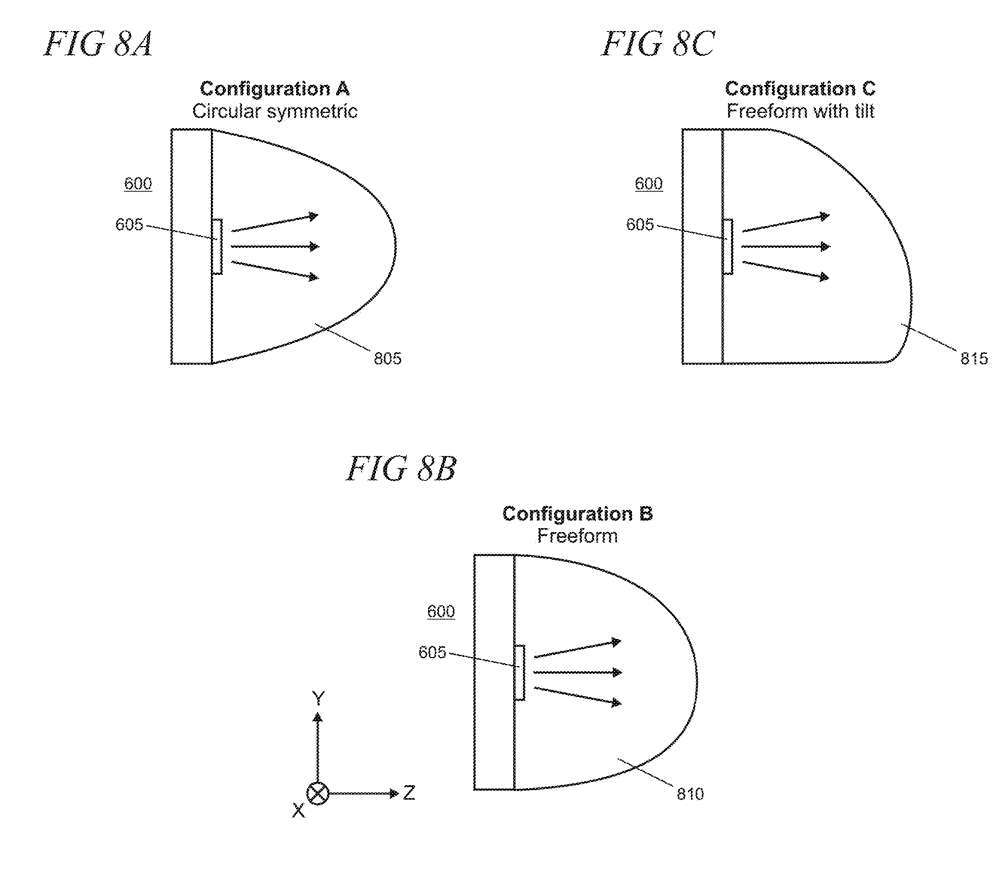
First Illustrative Structure FIG. 8A shows a structure for the microlens 805 (Structure A) in which the lens surface exhibits a circularly symmetrical shape. Second Illustrative Structure Figure 8B shows microlens 810 (Structure B) having a freeform lens surface shape
As a clarification, a "freeform lens surface" refers to a shape without an axis of rotational invariance. Therefore, the freeform lens exhibits different characteristics depending on its rotational position relative to the central axis of the Micro LED.
You can configure the freeform surface to optimize the beam shaping of the lens for almost all incident light rays. Aspheric optics can be viewed as a special case of freeform optics with rotationally invariant axes. Generally speaking, aspherical surfaces can have axes, while free-form surfaces can have no axes
Figure 8C shows a third illustrative structure of microlens 815 (Structure C) having a freeform lens surface shape. Structure C can be used for light manipulation of off-axis pixels. Its function is to tilt the microlens surface to match the angle of the emitted light to its CRA.
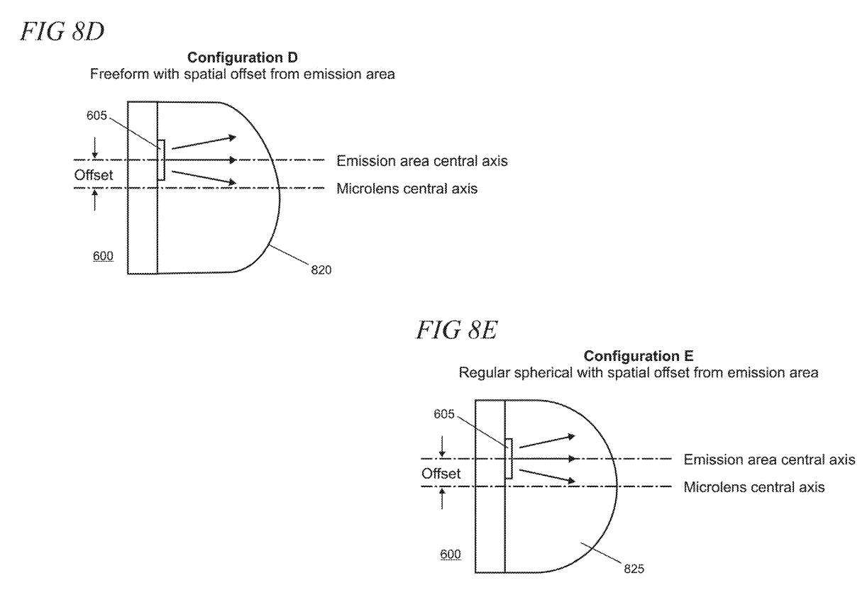
Figure 8D shows a fourth illustrative structure of microlens 820 (Structure D) having a freeform lens surface shape that provides CRA matching of off-axis pixels. Additionally, Structure D utilizes a non-coaxial spatial relationship in which the emitting area 605 of the Micro LED 600 is offset from the centerline of the microlens in the array plane.
Figure 8E shows a microlens 825 that has a regular spherical shape and utilizes an offset between the emission area of the Micro LED and the centerline of the microlens (Structure E).
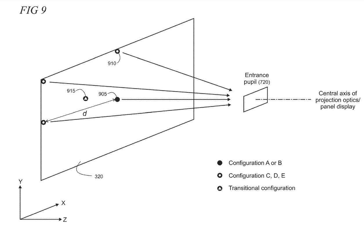
Figure 9 shows the distribution of different microlens configurations in the panel display 320. The microlens configuration of a particular pixel depends on its distance d on the central axis of the panel display. For pixels close to the central axis, you can choose to use microlens structure A or B with circular symmetry or free-form surface to obtain better results
For off-axis pixels, configurations C or D, respectively free shape and free shape with spatial offset, can be advantageously utilized to manipulate the rays emitted from the panel into the pupil 720 of the projection optics to match its respective CRA.
Thus, a given panel display can be used with one or more of the microlens configurations shown in Figure 8. For display pixels located between center and extreme off-axis positions, smooth transitions between configuration types can be achieved by implementing similar lens surface shapes and applying different spatial offsets calculated using linear interpolation between microlenses
The central axis of the microlens array corresponds to the central axis of the distal microlens array, so that the microlens array matches the axial and off-axis pixels of the panel display
The microlens array can be divided into multiple annular areas that are coaxial with the central axis of the display. The free-form surface shape of the microlens in each area can manipulate the principal ray angle of its corresponding pixel according to the principle described in the invention
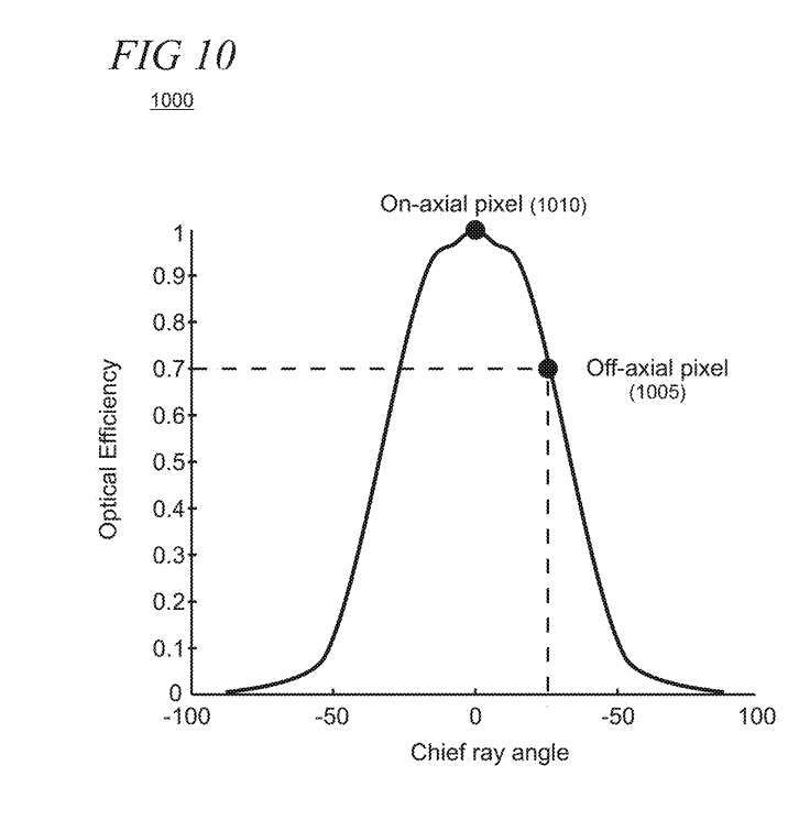
According to the principle of the present invention, the normalized optical efficiency of the panel display configured with microlenses is shown in Figure 1000 relative to the change in CRA. The results of Figure 10 can be seen
As shown in the figure, the optical efficiency of pixel 1005 with a CRA of 20 degrees is approximately 70% of that of pixel 1010 with a CRA of 0 degrees. The results compare favorably with certain conventional projection systems, where the optical efficiency of a 20 degree CRA pixel is only about 28% of that of a 0 degree CRA pixel.
Flowchart 1100 illustrates FIG. 11
for operating an optical display system to display a virtual image within a field of view.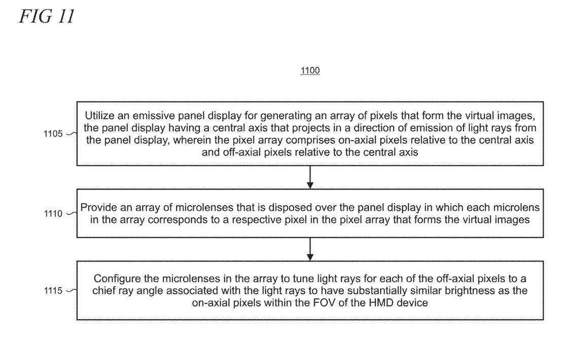
At 1105, an emissive panel display is utilized to generate an array of pixels that form a virtual image. The panel display has a central axis projected along a light emission direction of the panel display, and the pixel array includes upper-axis pixels relative to the central axis and off-axis pixels relative to the central axis.
At 1110, a microlens array disposed on the panel display is provided. Wherein, each microlens in the array corresponds to a respective pixel in the pixel array forming a virtual image.
At 1115, the microlens array is configured to tune the light to the chief ray angle relative to the off-axis pixels so that they have similar brightness to the on-axis pixels within the head-mounted display device's field of view
Related Patents: Microsoft Patent | Microlenses providing wide range chief ray angle manipulation for a panel display
The patent application "Microlenses providing wide range chief ray angle manipulation for a panel display" was submitted by Microsoft in March 2022 and was recently published by the US Patent and Trademark Office
The above is the detailed content of Microsoft explores AR/VR patents using microlens arrays for wide-range chief ray angle manipulation. For more information, please follow other related articles on the PHP Chinese website!


![[Web front-end] Node.js quick start](https://img.php.cn/upload/course/000/000/067/662b5d34ba7c0227.png)