According to reports, the Massachusetts Institute of Technology in the United States has recently developed a 3D printed precision plasma sensor. The device is low-cost and easy to manufacture. These digital devices can help scientists predict weather or study climate change. The plasma sensors, also known as "Retarded Potential Analyzers (RPAs)," are used by orbiting spacecraft such as Sputnik to determine the chemical composition of the atmosphere and the distribution of ion energy.
Semiconductor plasma sensors are manufactured through 3D printing and laser cutting processes. Since the process requires a dust-free environment, the semiconductor plasma sensors are expensive and require several weeks to complete. Complex manufacturing process. By comparison, MIT's latest plasma sensor takes just a few days to make and costs tens of dollars.
Because of its lower cost and speed of production, this new sensor is an ideal choice for CubeSats, which are low-cost, low-power and lightweight and are often used for communications and environmental monitoring in the Earth's upper atmosphere.
The research team developed a new type of plasma sensor using glass ceramic materials that are more elastic than traditional sensor materials such as silicon and thin film coatings. By using glass ceramics in the plastic 3D printing process, they can create complex shapes. sensors that can withstand the huge temperature fluctuations a spacecraft may encounter in low-Earth orbit.
Luis Fernando Velasquez-Garcia, senior author of the study and chief scientist at MIT’s Microsystems Technology Laboratory (MTL), said: “Additive manufacturing It will have a major impact in the field of future space hardware. Some people believe that when 3D printing some objects, they must accept lower performance, but we have now proved that this is not always the case." The latest research report was published recently Published in the Journal of Additive Manufacturing.
Plasma sensors were first used in space missions in 1959. They can detect the energy of ions or charged particles floating in plasma, which exists on the earth. A mixture of superheated molecules in the upper atmosphere. On orbiting spacecraft like CubeSats, plasma sensors can measure changes in energy and conduct chemical analyses, helping scientists predict weather or monitor climate change.
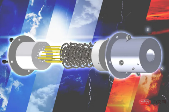
The sensor contains a series of charged grids filled with small holes. When the plasma passes through the small holes, electrons and other particles will be stripped away until only ions remain. When these ions generate an electric current, the sensor will Measure and analyze it.
The key to successful plasmonic sensor applications is an aligned grid of hole-like structures, which must be electrically insulating while being able to withstand drastic temperature swings. The researchers used a 3D-printable glass-ceramic material— —Vitrolite, which meets the above characteristics. It is reported that Vitrolite material first appeared in the early 20th century and was often used in colorful ceramic tile designs, becoming the most common material in Art Deco architecture.
The durable Vitrolite material can withstand temperatures up to 800 degrees Celsius without decomposing, while the polymer materials in integrated circuit-structured plasma sensors begin to melt at 400 degrees Celsius. "When workers build this sensor in a clean room, they won't have the same freedom to define the materials and structure and how they interact," Garcia said, "but that could lead to the latest developments in additive manufacturing." .”
The 3D printing process of ceramic materials usually involves laser bombardment of ceramic powder to fuse it into various shaped structures. However, due to the laser release With its high heat, this manufacturing process tends to roughen the material and create blemishes.
However, the MIT scientists used reductive polymerization in the manufacturing process, a process introduced decades ago that uses polymers or resins for additive manufacturing. In the reduction polymerization technology, the material is repeatedly immersed in a reduction tank containing Vitrolite liquid material. Once immersed, a layer of three-dimensional structure will be formed. After each layer of structure is formed, the material is cured with ultraviolet light. Each layer of the structure is only 100 microns thick. (equivalent to the diameter of a human hair), and eventually repeatedly immersed in the Vitrolite liquid material, a smooth, non-porous, complex ceramic structure will be formed.
In the digital manufacturing process, the manufacturing objects described in the design documents may be very complex. This high-precision design requires researchers to use a laser-cut mesh with a unique structure, which is installed on the plasma sensor housing after printing is completed. The small hole-like structure can be perfectly arranged to allow more ions to pass through it, thereby obtaining higher-precision measurement data.
Because the sensor is low-cost and fast to produce, the research team produced four unique design prototypes. One design prototype is particularly effective at capturing and measuring large-scale plasmas, especially for satellite orbital survey plasmas, and the other design prototype is well-suited for measuring extremely high-density, extremely cold plasmas, which is usually only possible in Ultra-precision semiconductor device measurements.
This high-precision design could enable 3D printed sensors to be used in fusion energy research or supersonic flight, and Garcia added that this fast 3D printing process could even lead to more innovations in satellite and spacecraft design.
Garcia said: "If you want to continue to innovate, you have to face failure and take the corresponding risks. Additive manufacturing is another way to make space equipment. We can make space devices, even if the process If it fails, it doesn’t matter because we can still make a new version quickly and cheaply and iterate on the design. For researchers, this is an ideal sandbox effect.”
It is reported that although Garcia is very satisfied with the latest design of the plasma sensor, he hopes to continuously improve the manufacturing process in the future and reduce the layer thickness or pixel size during the glass-ceramic cylinder polymerization process, thereby creating a more accurate sensor. complex device. In addition, the fully additive manufacturing process can make them continuously compatible with space manufacturing. He also hopes to explore the use of artificial intelligence to continuously optimize sensor design to adapt to specific application scenarios, such as significantly reducing sensor weight while ensuring structural stability.
The above is the detailed content of Scientists 3D print high-precision plasma sensors for satellites. For more information, please follow other related articles on the PHP Chinese website!


![[Web front-end] Node.js quick start](https://img.php.cn/upload/course/000/000/067/662b5d34ba7c0227.png)